
半导体Advanced Integration and Packaging

Current Service Inquiry

Hybrid Bonding

Plasma activation, room-temperature dielectric bonding, annealing Cu join-up, Cu/dielectric interface, bond strength, void control
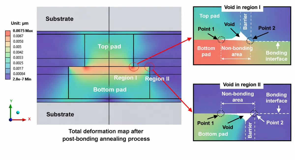
Results Display
Image is for technical case explanation only and does not represent company project results or a specific client case.

Calculation Purpose

Explain dielectric pre-bonding and Cu join-up across the three-step hybrid bonding process

Case Reference

Assessment of the Risk of Crack Formation at a Hybrid Bonding Interface Using Numerical Analysis

Hybrid bonding technology has recently emerged as a promising solution for advanced semiconductor packaging technologies. However, several reliability issues still pose challenges for commercialization. In this study, we investigated the possibility of crack formation caused by chemical mechanical polishing (CMP) defects and the misalignment of the hybrid bonding structure. Crack formation and thermomechanical stress were analyzed for two common hybrid bonding structures with misalignment using a numerical simulation. The effects of annealing temperature and dishing value on changes in the non-bonding area and peeling stress were systematically analyzed. The calculated peeling stresses were compared to the bonding strength of each bonding interface to find vulnerable regions prone to cracking. The non-bonding area in the bonding structure increased with a decreasing annealing temperature and an increasing dishing value. To achieve a sufficient bonding area of more than 90%, the annealing temperature should be greater than 200 °C. During the heating period of the annealing process, the SiCN-to-SiCN bonding interface was the most vulnerable cracking site with the highest peeling stress. An annealing temperature of 350 °C carries a significant risk of cracking. On the other hand, an annealing temperature lower than 250 °C will minimize the chance of cracking. The SiCN-to-SiO2 bonding interface, which has the lowest adhesion energy and a large coefficient of thermal expansion (CTE) mismatch, was expected to be another possible cracking site. During cooling, the SiCN-to-Cu bonding interface was the most vulnerable site with the highest stress. However, the simulated peeling stresses were lower than the adhesion strength of the bonded interface, indicating that the chance of cracking during the cooling process was very low. This study provides insights into minimizing the non-bonding area and preventing crack formation, thereby enhancing the reliability of hybrid bonding structures.

Read Article

Scan the QR code with WeChat for free consultation

If you are not sure which plan fits, send us your requirements.

Email: chengyankeji2026@163.com

Contact Us

WeChat QR Code

WeChat QR Code

Not sure which calculation fits? Share your material system and goal, and we will help assess the plan first.

Order now